On-site growth of perovskite nanocrystal arrays for integrated nanodevices

PubDate: July 2023
Teams: MIT
Writers: Patricia Jastrzebska-Perfect, Weikun Zhu, Mayuran Saravanapavanantham, Zheng Li, Sarah O. Spector, Roberto Brenes, Peter F. Satterthwaite, Rajeev J. Ram & Farnaz Niroui
PDF: On-site growth of perovskite nanocrystal arrays for integrated nanodevices
Abstract
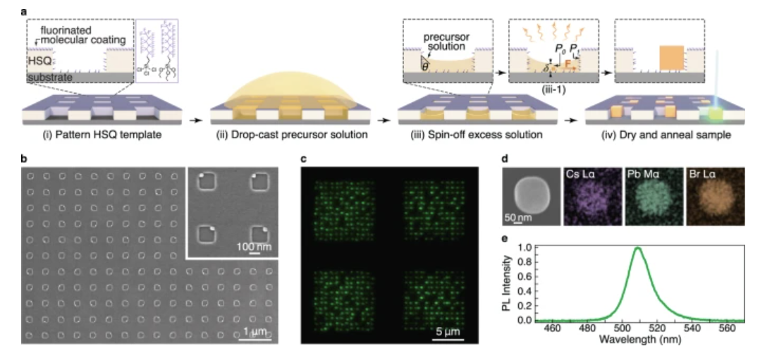
Despite remarkable progress in the development of halide perovskite materials and devices, their integration into nanoscale optoelectronics has been hindered by a lack of control over nanoscale patterning. Owing to their tendency to degrade rapidly, perovskites suffer from chemical incompatibility with conventional lithographic processes. Here, we present an alternative, bottom-up approach for precise and scalable formation of perovskite nanocrystal arrays with deterministic control over size, number, and position. In our approach, localized growth and positioning is guided using topographical templates of controlled surface wettability through which nanoscale forces are engineered to achieve sub-lithographic resolutions. With this technique, we demonstrate deterministic arrays of CsPbBr3 nanocrystals with tunable dimensions down to <50 nm and positional accuracy <50 nm. Versatile, scalable, and compatible with device integration processes, we then use our technique to demonstrate arrays of nanoscale light-emitting diodes, highlighting the new opportunities that this platform offers for perovskites’ integration into on-chip nanodevices.